- 您现在的位置:买卖IC网 > Sheet目录983 > HI5662EVAL2 (Intersil)EVALUATION PLATFORM HI5662
�� �
�
�HI5662EVAL2� Evaluation� Board� User’s� Manual�
�TM�
�Description�
�Application� Note�
�January� 1999�
�AN9823�
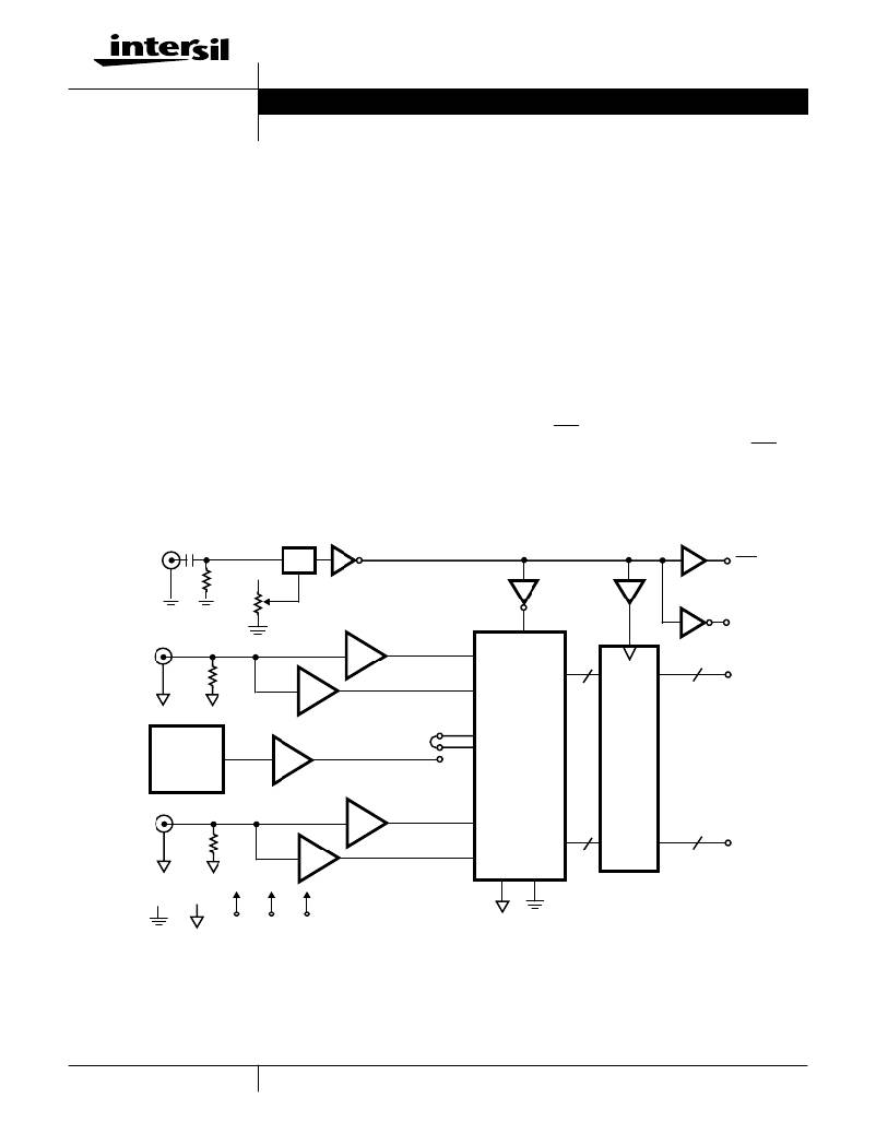
�The� HI5662EVAL2� evaluation� board� is� made� available� to� allow�
�the� circuit� designer� the� ability� to� evaluate� the� performance� of�
�the� Intersil� HI5662� monolithic� Dual� 8-bit� 60� MSPS� analog-to-�
�digital� converter� (ADC)� with� internal� voltage� reference.� As�
�shown� in� the� Evaluation� Board� Functional� Block� Diagram,� this�
�evaluation� board� includes� sample� clock� generation� circuitry,� a�
�single-ended� to� differential� analog� input� amplifier� configuration�
�for� both� the� I� and� Q� channel� inputs,� an� external� variable�
�voltage� reference� and� digital� data� output� latches/buffers.� The�
�buffered� digital� data� outputs� are� conveniently� provided� for�
�easy� interfacing� to� a� ribbon� connector� or� logic� probes.�
�The� sample� clock� generator� circuit� accepts� the� external�
�sampling� signal� through� an� SMA� type� RF� connector,� J3.� This�
�input� is� AC-coupled� and� terminated� in� 50� ?� allowing� for�
�connection� to� most� laboratory� signal� generators.� In� addition,�
�the� duty� cycle� of� the� clock� driving� the� A/D� converter� is� made�
�adjustable� by� way� of� a� potentiometer� so� that� the� effects� of�
�sample� clock� duty� cycle� on� the� HI5662� may� be� observed.�
�The� I� and� Q� channel� analog� input� signals� are� also� connected�
�through� SMA� type� RF� connectors,� J1� and� J2,� and� applied� to�
�single-ended� to� differential� analog� input� ampli?ers.� These�
�inputs� are� AC-coupled� and� terminated� in� 50� ?� allowing� for�
�connection� to� most� laboratory� signal� generators.� Also,�
�provisions� for� differential� RC� lowpass� ?lters� are� incorporated�
�on� the� output� of� the� differential� ampli?ers� to� limit� the�
�broadband� noise� going� into� the� HI5662� converter.�
�The� I� and� Q� channel� digital� data� output� latches/buffers�
�consist� of� a� pair� of� 74FCT2821� D-type� ?ip-?ops.� The� digital�
�data� output� interface� provides� both� phases� of� the� sampling�
�clock,� CLK� and� CLK,� so� that� the� digital� data� transitions� are�
�essentially� time� aligned� with� the� rising� edge� of� the� CLK�
�sampling� clock� or� time� aligned� with� the� falling� edge� of� the�
�CLK� sampling� clock� .�
�Evaluation� Board� Functional� Block� Diagram�
�SAMPLE�
�CLOCK�
�INPUT�
�J3�
�50� ?�
�+5V� D�
�BIAS�
�TEE�
�CLK�
�CLOCK�
�OUT�
�CLK�
�Q-CHANNEL�
�ANALOG�
�INPUT�
�J2�
�50� ?�
�G� =� +1�
�QI� IN� +�
�CLK�
�QD� 0� -QD� 7�
�8�
�D�
�Q�
�8�
�Q-CHANNEL�
�DIGITAL�
�DATA�
�(Q_IN)�
�ICL8069�
�G� =� -1�
�QI� IN� -�
�V� ROUT�
�OUTPUT�
�(QD0� -� QD9)�
�1.2V�
�BANDGAP�
�VAR�
�GAIN�
�+2.5V�
�V� RIN�
�VOLTAGE�
�REFERENCE�
�HI5662�
�I-CHANNEL�
�ANALOG�
�INPUT�
�J1�
�50� ?�
�G� =� +1�
�I� IN� +�
�ID� 0� -ID� 7�
�8�
�D�
�Q�
�8�
�I-CHANNEL�
�DIGITAL�
�DATA�
�(I_IN)�
�DGND�
�AGND�
�+5V� D�
�+5V� A�
�G� =� -1�
�-5V� A�
�I� IN� -�
�OUTPUT�
�(ID0� -� ID9)�
�3-1�
�1-888-INTERSIL� or� 321-724-7143�
�|�
�Intersil� and� Design� is� a� trademark� of� Intersil� Corporation.�
�|�
�Copyright�
�?� Intersil� Corporation� 2000�
�发布紧急采购,3分钟左右您将得到回复。
相关PDF资料
HI5714EVAL
EVALUATION PLATFORM HI5714
HI5728EVAL1
EVALUATION PLATFORM TQFPHI5728
HI5731-EVS
EVALUATION PLATFORM SOIC HI5731
HI5741-EVS
EVALUATION PLATFORM HI5741
HI5760EVAL1
EVALUATION PLATFORM SOIC HI5760
HI5762EVAL2
EVALUATION MOD FOR HI5762 AMP
HI5767EVAL1
EVALUATION PLATFORM HI5767
HI5767EVAL2
EVALUATION PLATFORM HI5767
相关代理商/技术参数
HI5662IN
制造商:未知厂家 制造商全称:未知厂家 功能描述:Converter IC
HI5667
制造商:INTERSIL 制造商全称:Intersil Corporation 功能描述:8-Bit, 60MSPS A/D Converter with Internal Voltage Reference
HI5667/6CA
制造商:Rochester Electronics LLC 功能描述:A/D, 8-BIT,60MSPS,COM TEMP,28 SSOP,TTL/CMOS (HI5767/6, 10- - Bulk
HI5667/6CB
制造商:Rochester Electronics LLC 功能描述:- Bulk
HI5667EVAL2
制造商:Rochester Electronics LLC 功能描述:- Bulk
HI5675
制造商:INTERSIL 制造商全称:Intersil Corporation 功能描述:8-Bit, 20MSPS, Flash A/D Converter
HI5675_03
制造商:INTERSIL 制造商全称:Intersil Corporation 功能描述:8-Bit, 20MSPS, Flash A/D Converter
HI5675JCB
制造商:Rochester Electronics LLC 功能描述:- Bulk